
PCB Design & Development
What is PCB ?
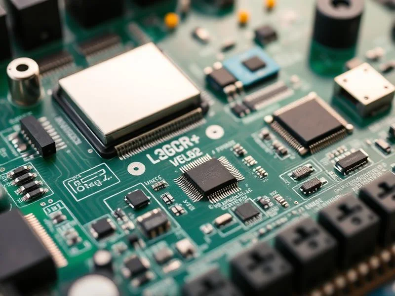
A Printed Circuit Board (PCB) is a flat board used to mechanically support and electrically connect electronic components using conductive copper tracks. It serves as the foundation of most electronic devices, allowing components like resistors, capacitors, and integrated circuits to work together efficiently. PCBs help improve reliability, reduce wiring complexity, and ensure compact, organized, and high-performance electronic systems.
Benefits of PCB Design & Development
Custom PCB Design
The creation of PCBs tailored to specific application needs, ensuring optimal performance, reliability, and efficient integration into electronic systems.
Schematic Capture & Simulation
Involves creating accurate circuit diagrams and testing their behavior virtually before PCB layout. This process helps identify errors early, verify performance, and ensure reliable and efficient circuit operation.
PCB Layout & Routing
Involves placing components and designing copper traces to ensure proper signal flow, minimal interference, and efficient thermal management for reliable circuit performance.
Prototyping & Fabrication
Involve converting the final PCB design into a physical board for testing and validation. This stage ensures the design performs as expected before moving into full-scale production.
Testing & Validation
Ensures the PCB functions correctly and reliably by checking performance and detecting defects before final production.